久久精品国产亚洲av麻豆长发,欧美黄色大片一区二区三区,国产精品久久久久久久久蜜,亚洲香蕉一区二区在线观看,精品国产一区二区三区欧美,国产三级av在线免费观看,www亚洲精品久久久乳网站,日韩欧美亚洲国产中文字幕网

CIOE China Optoelectronic Expo is coming with great enthusiasm. Unicon invites you to join this grand event!

2025-09-02 15:23:22 admin
光博會-頭圖.png

This year's CIOE China Optoelectronic Expo has gathered over 3,700 high-quality exhibitors from more than 30 countries and regions around the world. As a comprehensive exhibition covering the entire optoelectronic industry chain, it encompasses sections such as information and communication, precision optics, camera technology and applications, lasers and intelligent manufacturing, infrared, ultraviolet, intelligent sensing, and new displays. Uniconon will participate in the 25th China Optoelectronic Expo!

We sincerely invite you to visit the exhibition


Unicon will bring a variety of film thickness gauges to the exhibition

Looking forward to discussing with you on-site the various applications of film thickness measurement!

There are more fun interactions on site, waiting for you to win prizes

Picture Keywords

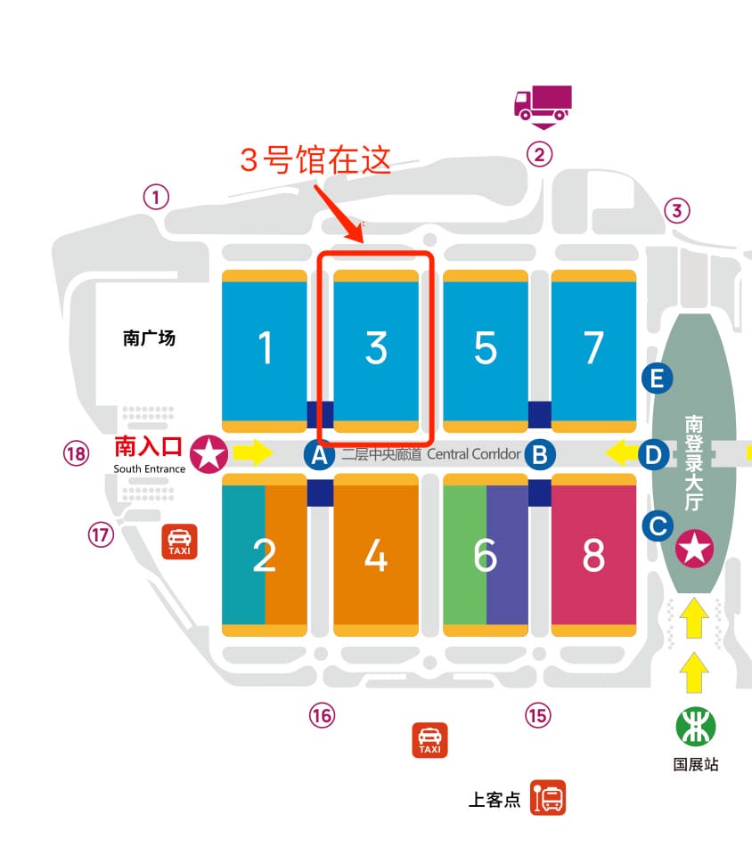
Unicon is in Hall 3 of the Shenzhen International Convention and Exhibition Center

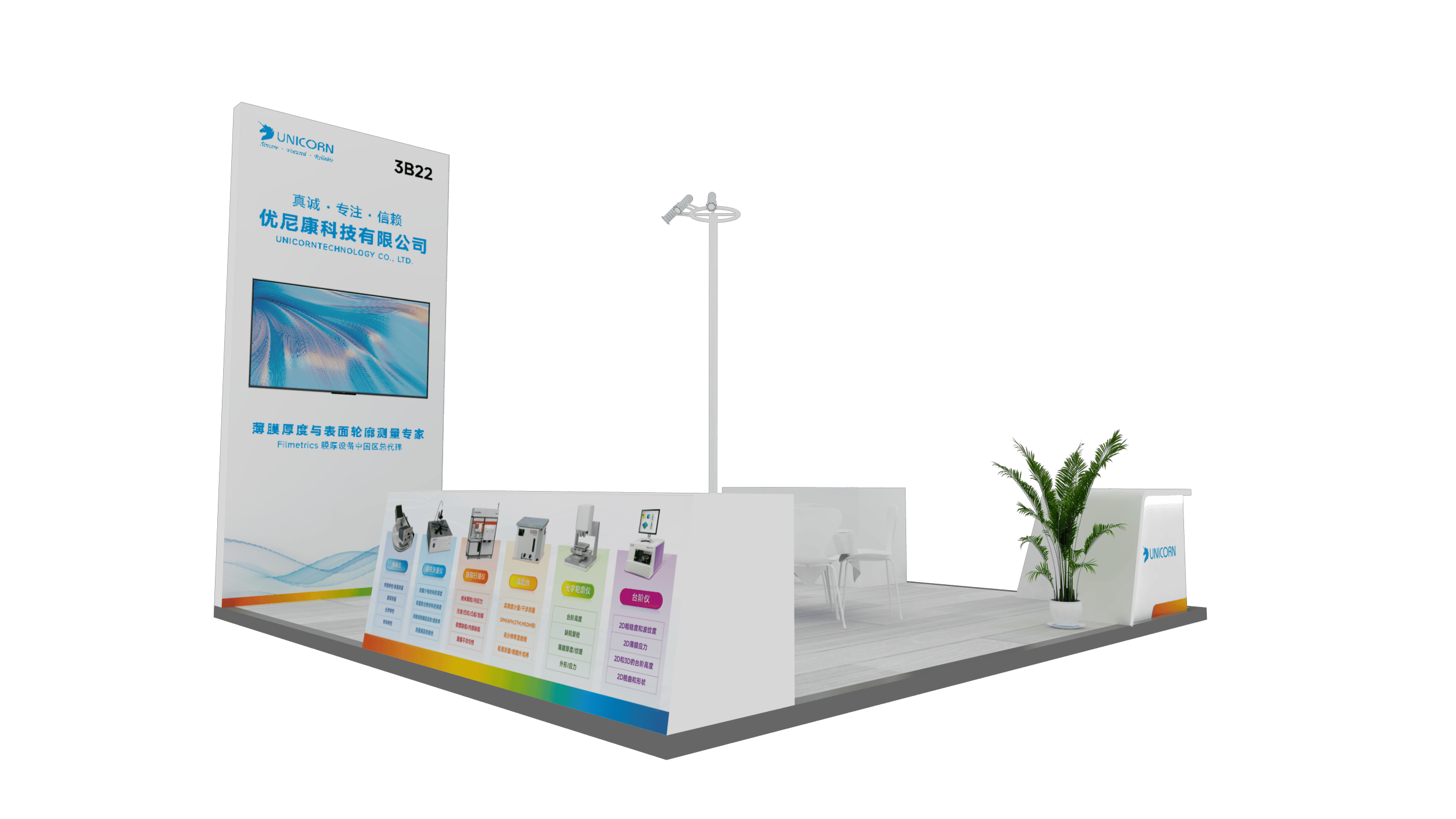
Preview image of the exhibition hall
Picture Keywords

Unicon booth3B22

Booth Preview

5.png

More exciting activities are gradually being unlocked

100% winning probability? Fun prizes? Participate and get it!

Picture Keywords

Exhibition equipment

Picture Keywords

F50 Film thickness Measuring instrument

The F50 can achieve maximum straightness very simplyThickness distribution map of the sample film with a diameter of 450 millimeters. The r-θ polar coordinate moving platform is adoptedIt can quickly locate the required test points and obtain the test thickness in real time, approximatelyTest two points per second.

Related applicationsSemiconductor manufacturing (photoresist, oxides/nitrides /SOI, wafer backside grinding); LCD liquid crystal display (polyimide, ITO transparent conductive film); Optical coating (hard coating, anti-reflection layer); MEMS micro-electromechanical systems (photoresist, silicon-based film layers).

Picture Keywords
Picture Keywords

P7 Step gauge

The P-7 can perform 2D and 3D measurements of step height, roughness, warpage and stress, and its scanning can reach 150mm without image stitching.

Related applicationsFilm/thick film steps Etching depth measurement Photoresist/photoresist step Flexible film Characterization of surface roughness/flatness; Surface curvature and contour analysis; 2D stress measurement of thin films Surface structure analysis 3D contour imaging of the surface Defect characterization and defect analysis.

Picture Keywords
Picture Keywords


F54-XY-200 Film Thickness Measuring instrument

The F54-XY-200 is equipped with an automated film thickness plotting system.With the advanced spectral reflection system of the F54-XY-200, the film thickness of samples up to 200 x 200mm can be measured quickly and easily.

Related applicationsSemiconductor manufacturing (photoresist, oxides/nitrides /SOI, wafer backside grinding); LCD liquid crystal display (polyimide, ITO transparent conductive film); Optical coating (hard coating, anti-reflection layer); MEMS micro-electromechanical systems (photoresist, silicon-based film layers).

Picture Keywords


Picture Keywords


Profilm3D White Light Interference Optical Profilometer

Profilm3D employs the most advanced vertical interference scanning (WLI) and high-precision phase interference (PSI) technologies. Achieve sub-nanometer surface morphology research with strong cost performance.

Related applicationsRoughness measurement Three-dimensional topography characterization Measurement of step height

Picture Keywords
Picture Keywords

FS-1 multi-wavelength ellipsometer

The Film Sense FS-1 multi-wavelength ellipsometer adopts a long-life LED light source and a non-moving component ellipsometer detector, enabling reliable film measurement in a compact ellipsometer with simple operation.

Related applicationsSilicon dioxide and nitrides, high dielectric and low dielectric materials, amorphous and polycrystalline materials, silicon films, photoresists.High and low index films, such as SiO2, TiO2, Ta2O5, MgF2.TCO (such as ITO), amorphous silicon thin films, organic thin films (OLED technology), etc


Schedule a Free Sample Analysis Today

Contact us to get your customized sample measurement solution.

PRECISION THIN FILM MEASUREMENT EXPERT

HOME 广宗县| 临西县| 威远县| 胶州市| 赤城县| 嵊州市| 七台河市| 望都县| 大关县| 庆阳市| 邹城市| 句容市| 隆尧县| 探索| 桃园县| 利辛县| 维西| 张家川| 安阳市| 石台县| 边坝县| 措勤县| 辽阳市| 遵义县| 礼泉县| 社旗县| 忻州市| 同江市| 华阴市| 达拉特旗| 山阳县| 阆中市| 城固县| 邻水| 凌海市| 贡山| 调兵山市| 上高县| 江都市| 玉门市| 缙云县|