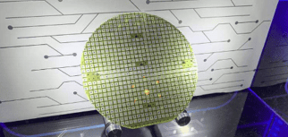
In SiC semiconductors Film thickness measurement solution Unikang Technology Co., LTD
Directory
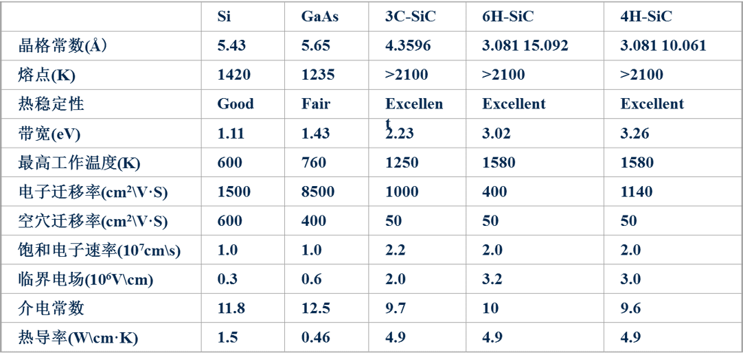
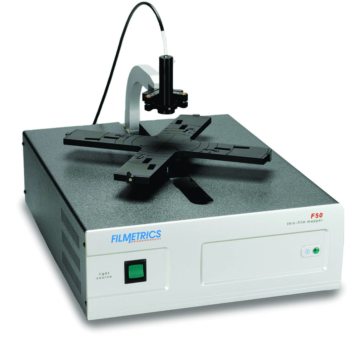
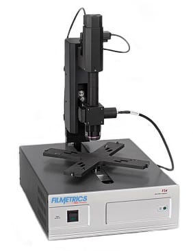
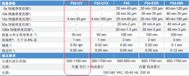
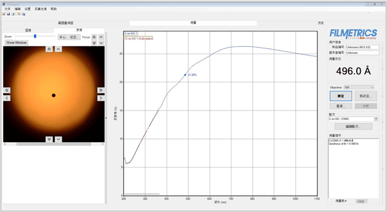
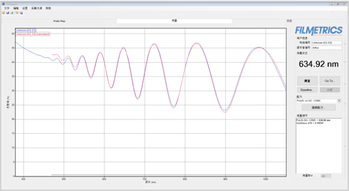
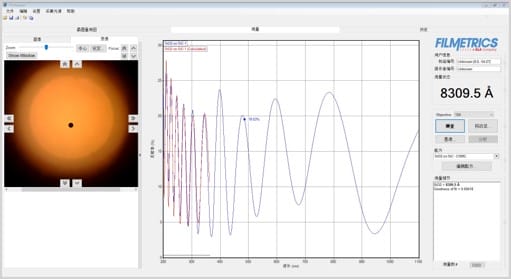
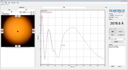
01 Overview of SiC Semiconductor Materials 02 The advantages of SiC material 03 Types of SiC devices 04 Application of SiC Semiconductor 05 SiC semiconductor manufacturer 06 Measurement requirements for SiC semiconductors 01 With the maturation of the first and second generation semiconductor materials, the Si power devices currently in large-scale use have reached their performance bottlenecks. The improvement of the operating frequency, power, heat resistance temperature, energy efficiency, resistance to harsh environments and miniaturization of Si power devices is facing insurmountable bottlenecks. In modern technology, more and more fields require third-generation semiconductors with high frequency, high power, high temperature resistance and good chemical stability. As an outstanding representative of third-generation semiconductors, SiC (Silcon carbide) is attracting more and more attention. As a new type of semiconductor material, SiC has become an important semiconductor material for manufacturing short-wavelength optoelectronic devices, high-temperature devices, radiation-resistant devices and high-power/high-value electronic devices due to its excellent physical, chemical and electrical properties. Especially when applied under harsh and severe conditions, the characteristics of SiC devices far exceed those of Si devices and GaAs devices. Therefore, SiC devices and various sensors have gradually become one of the key components and are playing an increasingly important role. Since the 1980s, especially since the first SiC substrate wafer entered the market in 1989, SiC devices and circuits have developed rapidly. In some fields, such as light-emitting diodes, high-frequency high-power and high-voltage devices, SiC devices have been widely applied commercially. 02 Sic silicon carbide materials generally have the following advantages: 1. High impact field strength 2. High thermal conductivity 3. It has strong high-temperature oxidation resistance 4. Good wear resistance 5. Stable chemical properties 6. High saturation and electron drift rate Comparison of relevant parameters of SiC with Si and GaAs 03 Silicon carbide devices mainly include power diodes and power switch tubes. Power diode Power switch tube 04 Silicon carbide semiconductor devices, with their high-frequency, high-efficiency and high-temperature characteristics, are particularly suitable for applications with strict requirements for efficiency or temperature. It can be widely applied in fields such as solar inverters, on-board power supplies, motor controllers for new energy vehicles, UPS, charging piles, and power supplies. 05 Foreign manufacturers Domestic manufacturers Infineon of Germany Zhuzhou CRRC Times Semiconductor Cree Company of the United States Qidi New Materials (Wuhu GE Wuxi China Resources Shanghua Technology Rohm Corporation of Japan ... 06 Common types of film thickness tests in SiC semiconductor process measurement: -SI (1000-20000A) SiNx (100-4000A) SiO2 (30-10000A) USG(1000-20000A) C film (100-2000A BPSG (1000-20000A) POLY (1000A-20000A) Match the product model F50-UV F54-UV Measurement parameters Measurement data C on SiC POLY on SiC SiO2 on SiC SiNx on SiC USG on SiC BPSG on SiC The author of this article Hu Shudong Sales Manager of East China Region With over a decade of experience in the film measurement industry, I have extensive expertise in providing solutions for film measurement. It has solved the originally rather thorny problems in the microfluidic chip industry, such as the need to measure the morphology and depth of flow channels. There will be a time when the strong wind breaks through the waves and the sail is hoisted high to cross the vast sea We have been deeply involved in the film measurement industry for over a decade. No matter what problems you have in film measurement, our technical experts can provide you with valuable advice or solutions. Welcome to call us. We are very glad to discuss your application issues with you. Consultation hotline: 400-186-8882 E-mail: info@unicorn-tech.com Unikang Technology Co., LTD Yiying Technology (Shanghai) Co., LTD