久久精品国产亚洲av麻豆长发,欧美黄色大片一区二区三区,国产精品久久久久久久久蜜,亚洲香蕉一区二区在线观看,精品国产一区二区三区欧美,国产三级av在线免费观看,www亚洲精品久久久乳网站,日韩欧美亚洲国产中文字幕网

[Exhibition Information] Unicon invites you to meet at the Shanghai New International Expo Center

2025-09-02 15:23:22 admin
邀請(qǐng)函頭圖.png

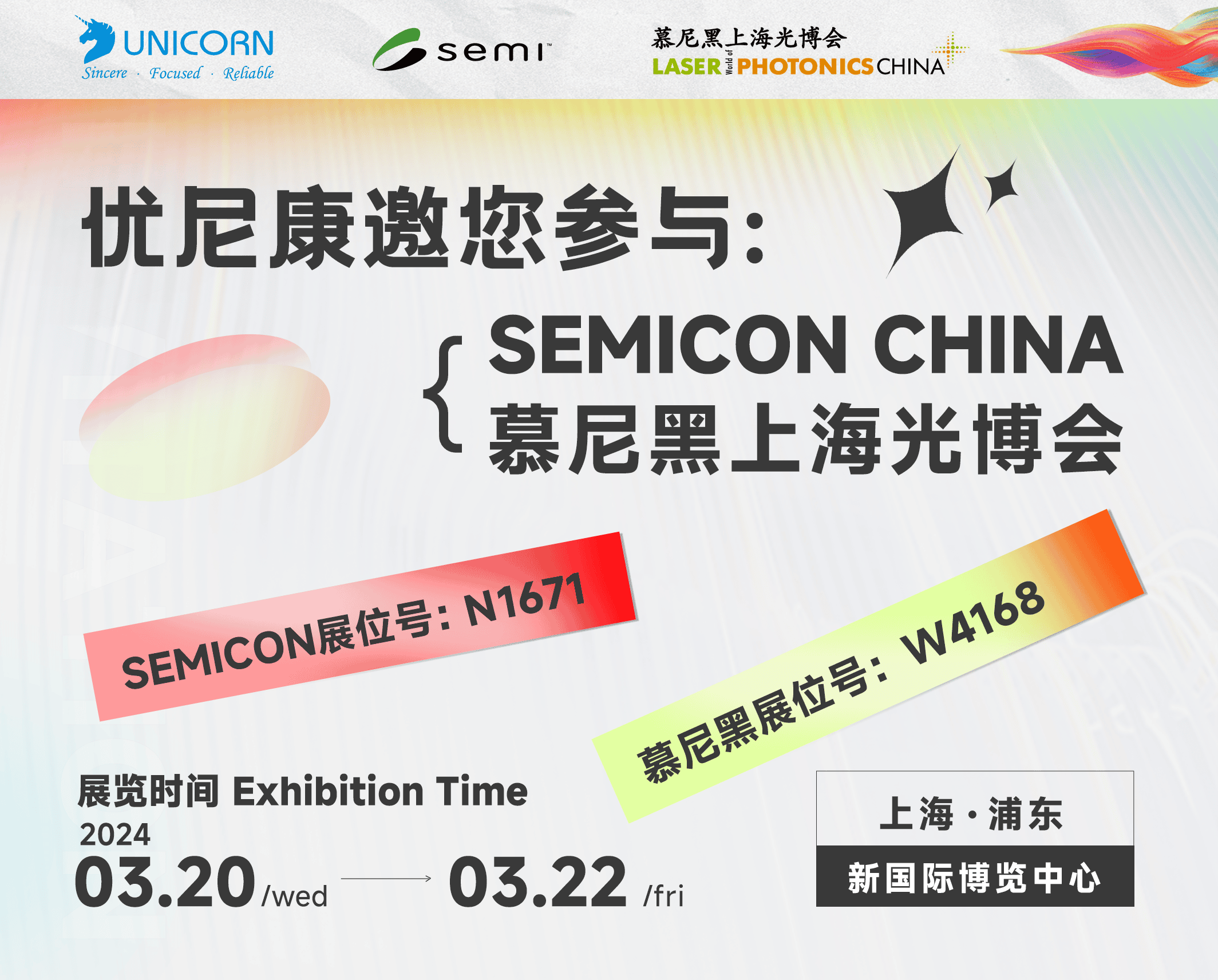
The 2024 SEMICON CHINA and the Laser World of Photonics China will be held concurrently at the Shanghai New International Expo Center. Uniconon will bring multiple devices to participate in this grand event. You can scan the QR code below the article to make an online reservation and sign up in advance. We look forward to meeting you on the spot. We have prepared many exquisite small gifts for you to collect.

Picture Keywords


SEMICON CHINA

Booth NumberHall N1, Room 1671


The Laser World of Photonics China in Shanghai

Booth NumberHall W4, Room 4168

Picture Keywords
Picture Keywords


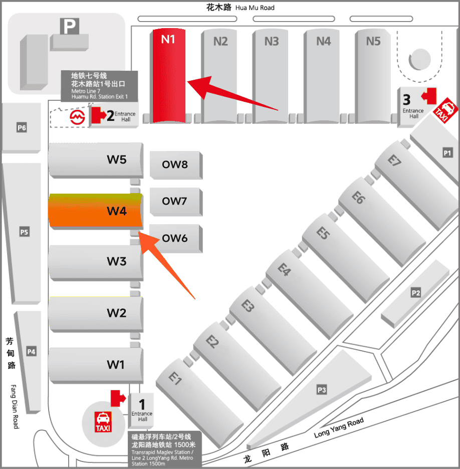
Exhibition hall floor plan

Picture Keywords

SEMI Exhibition Reservation

Picture Keywords

Munich Exhibition Reservation

You can scan the QR code above to make an appointment for a visit

Looking forward to your arrival!!

圖層 11.png

Exhibition equipment

高清大圖 (1).jpg

Filmetrics F50 Film Thickness Measuring instrument

The F50 can very simply obtain the thickness distribution map of sample films with a maximum diameter of 450 Youdaoplaceholder0. By using the r-θ polar coordinate moving platform the required test points can be quickly located and the test thickness can be obtained in real time, approximately 2 points per second.

Related applicationsSemiconductor manufacturing (photoresist, oxides/nitrides /SOI, wafer backside grinding); LCD liquid crystal display (polyimide, ITO transparent conductive film); Optical coating (hard coating, anti-reflection layer); MEMS micro-electromechanical systems (photoresist, silicon-based film layers).


資源 1.png

Bowman XRF Coating Thickness gauge

It has a 12 x12-inch measurable area superior to similar products on workpieces with a height not exceeding 9 inches. The automatic multi-collimator allows for the selection of spot sizes to accommodate various feature sizes. The zoom camera allows for measurements within a focal length range of 0.25 inches to 3.5 inches.


Related applicationsTest of refractive index extinction coefficient of materials Testing of the thickness of the natural oxide layer on silicon wafers Test of optical constants of photoresist Measurement of metal thickness on silicon in the back-end packaging of semiconductors


Picture Keywords

Lumina AT2 Defect Detector

The film defect detector enables full surface scanning and imaging of sub-nanometer film coatings, nanoparticles, scratches, pits, protrusions, stress points and other defects.


Related applicationsAll types of defects; Thin and thick substrate; Transparent and opaque substrates; Dielectric coating Metal coating; Bonded silicon wafers Development and online production


More models are waiting for you to experience on site...


Schedule a Free Sample Analysis Today

Contact us to get your customized sample measurement solution.

PRECISION THIN FILM MEASUREMENT EXPERT

HOME 南康市| 静宁县| 阜阳市| 乌什县| 屏南县| 呈贡县| 新化县| 龙州县| 磴口县| 民和| 庆城县| 许昌市| 调兵山市| 鄂州市| 晋宁县| 孝昌县| 上虞市| 东丰县| 梅州市| 吉林省| 安顺市| 潼南县| 沁源县| 武胜县| 怀柔区| 广德县| 册亨县| 汽车| 通山县| 都匀市| 萨嘎县| 噶尔县| 中方县| 安吉县| 新源县| 扎囊县| 上栗县| 西吉县| 夏河县| 石狮市| 灵石县|